
 Inggris
 中文简体
中文简体 Русский
 Español
 Português
 Türkçe
 العربية
 Deutsch
 Polski
 Italiano
 Français
 한국어
한국어 ไทย
ไทย Tiếng Việt
 日本語
日本語
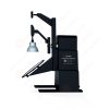
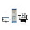
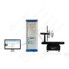

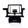
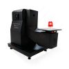
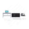











Sistem Uji ESD CDM
Pengguna manual
berlaku LISUN models: ESD-CDM
1. Pemahaman Dasar tentang Peralatan
1.1 Ikhtisar Produk
The ESD-CDM (Charged Device Model) CDM ESD Test System is a high-precision immunity test instrument specifically designed for “charged device contact discharge” scenarios involving semiconductor devices during production, transportation, and assembly. Its core function is to simulate the transient discharge process that occurs when a semiconductor device—which has become charged (e.g., through triboelectric charging or induced charging)—comes into contact with a grounded object. By precisely controlling parameters such as discharge voltage and current waveforms, it evaluates the device’s tolerance to this type of “latent electrostatic shocks,” enabling the early detection of risks such as internal circuit burnout and functional failure. It provides a testing basis for the reliability design, mass production quality inspection, and international compliance certification of semiconductor devices.
This system features an integrated “charge injection–contact discharge” design and is equipped with a high-precision charge measurement module, with a discharge voltage error of ≤±3%; It is compatible with fixtures for mainstream semiconductor packages such as DIP, SOP, QFP, and BGA. Equipped with a touchscreen display in both Chinese and English, it supports one-click configuration of test parameters, automated control of the discharge process, and real-time storage of test data, meeting the semiconductor industry’s requirements for high precision and high compatibility in testing.
1.2 Standar yang berlaku
This equipment fully complies with the following domestic and international CDM electrostatic discharge testing standards:
| Nomor Standar | Judul Standar |
|---|---|
| ANSI/ESDA/JEDEC JS-002-2014 | Electrostatic Discharge (ESD) Sensitivity Testing—Charged-Device Model (CDM)—Component Level |
| IEC 60749-28: 2022 | Semiconductor Devices—Mechanical and Climatic Test Methods—Part 28: Electrostatic Discharge (ESD) Sensitivity Testing—Charged-Device Model (CDM) |
| AEC-Q100-011 | Charged Device Model (CDM) Electrostatic Discharge Test |
| EIA/JESD22-C101 | Test Method for Electrostatic Discharge Sensitivity Testing—Charged-Device Model (CDM) |
| ANSI/ESDS 5.3.1-2009 | Electrostatic Discharge Sensitivity Testing – Charged Device Model (CDM) – Component Level |
| JEITA ED-4701/300 Test Method 305 | Charged Device Model Electrostatic Discharge (CDM/ESD) |
| GB / T 4937.28-2024 | Semiconductor Devices—Mechanical and Climatic Test Methods—Part 28: Electrostatic Discharge Sensitivity Testing—Charged Device Models (Equivalent to IEC 60749-28:2022) |
1.3 Principles of the CDM Discharge Model
The Charged Device Model (CDM) simulates the physical process by which a semiconductor device accumulates static electric charge and then discharges it through contact between its pins and a grounded conductor. The device becomes charged through an induced high-voltage electric field, and when the device’s pins come into contact with a ground probe, the stored charge is rapidly discharged within nanoseconds, forming a discharge current pulse with a high peak and a fast rising edge. This pulse exerts a stress on the device’s internal gate oxide layer and metal interconnects, thereby evaluating the device’s electrostatic discharge (ESD) tolerance.
2. Tindakan Pencegahan Keamanan
2.1 Persyaratan Lingkungan Kerja
Operating temperature: 15°C to 35°C; operating relative humidity: 30% to 60%. Do not use in environments with high humidity or condensation to prevent high-voltage arcing.
There must be no strong electromagnetic interference, no sources of vibration, no flammable or explosive materials, and no corrosive gases in the surrounding area.
Place it on a stable work surface; avoid tilting or inverting it, and keep it away from sources of vibration.
The distance between the equipment and walls or surrounding structures (such as other test equipment or shelving) must be at least 500 mm to facilitate pemeliharaan; setidaknya 1000 mm of space must be left in front of the equipment to ensure smooth operation, with no obstructions in the surrounding area.
2.2 High-Voltage Safety Standards
2.2.1 Pemeriksaan Keamanan
Pastikan catu daya kompatibel dengan peralatan, pastikan catu daya terhubung ke ground dengan benar, dan periksa apakah kabel ground tidak rusak atau longgar;
Grounding Requirements: The host unit’s protective grounding terminal (PGND) must be connected to ground; the grounding resistance must be ≤4Ω; the grounding cable must be securely connected, with no looseness or breaks.
2.2.2 Persyaratan Keselamatan untuk Prosedur Operasional
Operators must undergo professional training and be familiar with this manual and the relevant standards. Non-professionals are prohibited from operating or disassembling the equipment. The equipment contains high-voltage circuits; opening the cover may pose an electric shock hazard. Contact the manufacturer’s technical staff for repairs;
Once the equipment is powered on, do not touch the test bench, high-voltage cables, discharge probes, or other related components to prevent electric shock;
Operators should ensure their hands are dry and free of metal jewelry; it is recommended that they wear insulated gloves while working;
Do not eat or drink during the test to prevent accidents caused by electric shock;
Jika melibatkan beberapa orang, tetapkan peran dan tanggung jawab dengan jelas, dan konfirmasikan satu sama lain sebelum memulai pengujian untuk menghindari kesalahan.
2.3 Standar Keselamatan Peralatan
Before connecting or disconnecting high-voltage cables, you must turn off the main unit’s power and wait at least 5 minutes to ensure that the internal capacitors are completely discharged;
When inserting a high-voltage plug into an outlet, align it with the positioning pins. Never force the plug into the outlet if it is not properly aligned, to avoid damaging the internal copper pins;
If you discover damage to high-voltage cables or loose connectors, stop using the product immediately and contact customer service to have them replaced;
Do not suddenly cut off the power or unplug or plug in the high-voltage connector while the equipment is running, to avoid damaging the high-voltage module;
Do not scratch the touchscreen with hard objects, and do not press the screen with sharp objects;
Avoid bumping the equipment during testing to prevent the device under test from shifting, which could cause the test to fail or damage the probes.
2.4 Lainnya
Untuk hal-hal yang tidak tercakup dalam panduan ini, harap berhati-hati atau hubungi kami.
3. Gambaran Umum Peralatan dan Pengkabelan
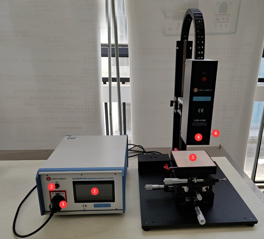
3.1 Tampak depan
Lihat Gambar 3-1.
| Jumlah | Note |
|---|---|
| Simulator Pelepasan Elektrostatis | |
| ① | Touchscreen |
| ② | High-Voltage Indicator Light |
| ③ | High-voltage connection. Lift the positioning pin, align the groove in the discharge tower’s high-voltage plug with the positioning pin, and slowly insert it all the way to the bottom. Then lower the positioning pin to lock the high-voltage plug in place. |
| CDM Electrostatic Discharge Tower | |
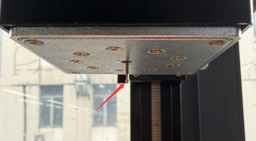
| ④ | Probe lift frame; the probe mounting location is directly opposite the test bench, as shown in Figure 3-2. |
| ⑤ | Standard test stand, adjustable for both position and height |
| ⑥ | BNC connector; use a coaxial cable to connect to an oscilloscope to view the output waveform. Note: Make sure the oscilloscope has a sufficient range, or use an attenuator to prevent damage to the oscilloscope. |
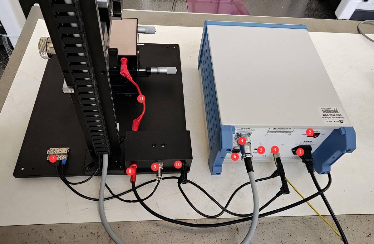
3.2 Tampilan belakang
Lihat Gambar 3-3.
| Jumlah | Note |
|---|---|
| Simulator Pelepasan Elektrostatis | |
| ① | Soket kabel daya (dengan sekering) untuk menghubungkan perangkat ke sumber daya yang sesuai. |
| ② | Saklar daya |
| ③ | PGND: Protective ground terminal; connect to earth using a ground wire. |
| ④ | Connecting the Signal Cables to the Discharge Tower |
| ⑤ | USB port: Can be used to connect a USB mouse to control the touchscreen, or to connect a USB flash drive to update the software. |
| ⑥ | LAN port, spare |
| CDM Electrostatic Discharge Tower | |
| ⑦ | Grounding busbar: Connect the ground wire from the probe lifting frame to the grounding busbar, and then use a wire to connect the grounding busbar to the protective grounding terminal on the back of the Electrostatic Discharge Simulator. |
| ⑧ | High-Voltage Line Connection |
| ⑨ | Signal Line Connections |
| ⑩ | Connect the test bench ground wire to the protective ground terminal on the back of the Electrostatic Discharge Simulator. |
| ⑪ | High-Voltage Cable Connections on the Test Stand |
3.3 Replacing the Discharge Tower
This Electrostatic Discharge Simulator can be connected to discharge towers used for various tests. If you need to replace the discharge tower for testing, please follow the operating procedures below strictly.
| petunjuk | Note |
|---|---|
| ① | Verify that the Electrostatic Discharge Simulator is in the “Test Stopped” state, then shut it down. |
| ② | Disconnect all cables connecting the original discharge tower to the Electrostatic Discharge Simulator. |
| ③ | Connect all the cables between the new discharge tower and the Electrostatic Discharge Simulator. |
| ④ | Turn on the computer and run the new test. |
4. Pengantar Program Layar Sentuh
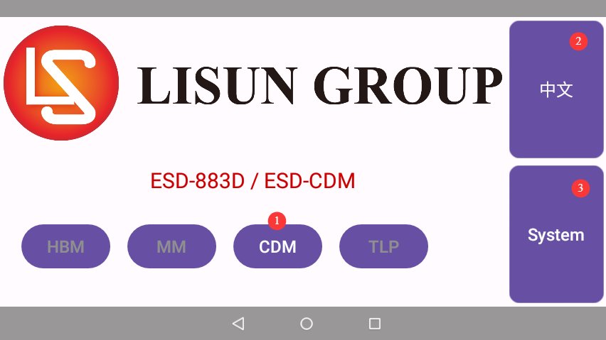
4.1 Layar awal
Lihat Gambar 4-1.
| Jumlah | Note |
|---|---|
| ① | When the CDM discharge tower is connected to the host, “CDM Available” will be displayed; click it to enter the CDM test interface. |
| ② | Beralih antara Bahasa Mandarin dan Bahasa Inggris |
| ③ | Halaman Informasi Produk |
4.2 CDM Test Interface
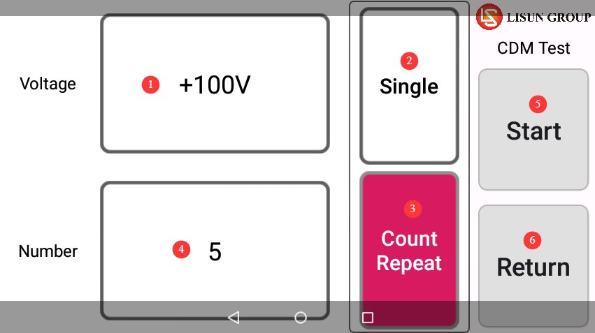
Lihat Gambar 4-2.
| Jumlah | Note |
|---|---|
| ① | The test voltage and polarity can be set |
| ② | If you want to run a single test, select “Single Test.” |
| ③ | If you want to run continuous testing, select “Continuous Testing.” |
| ④ | You can set the number of tests; only consecutive tests are allowed. |
| ⑤ | Start/Stop Test |
| ⑥ | Kembali ke Layar Beranda |
5. CDM Electrostatic Discharge Testing
5.1 Preliminary Commissioning of the Test Bench Location
5.1.1 Placement Requirements for the Device Under Test
Operators should wear antistatic wristbands and antistatic clothing to prevent static electricity from the human body from damaging the devices under test; place the semiconductor devices under test with their pins facing upward in the center of the isolation plate,
5.1.2 Test Bench Commissioning
First, disconnect the high-voltage connection cables and place them on an insulated work surface. Then, refer to Section 4.2 to begin the test. Lower the probe at the standard speed. Based on the probe’s position as it descends, adjust the test stand’s height and horizontal alignment so that the probe makes just enough contact with the target pin upon reaching the bottom. Observe the contact status to avoid damaging the device pins due to excessive pressure. Once the adjustments are complete, stop the test and reconnect the high-voltage cable.
5.2 Recommended Standard Test Parameters
In accordance with the ANSI/ESDA/JEDEC JS-002-2014 standard, the recommended parameters for routine testing are as follows: Discharge voltage: Select based on device class—Class 0 (<250 V), Class 1 (250 V to <500 V), Class 2 (500 V to <1000 V), Class 3 (≥1000 V); Discharge polarity: Test once for both positive and negative polarities; Number of discharges: At least 3 discharges per pin.
5.3 Start/Stop Test
Set the test parameters as described in Sections 4.2 and 5.2, and start the test. If any abnormalities occur during the test, press the stop button to halt the test, make the necessary adjustments, and try again. After the test is complete, ensure that any internal residual charge is completely discharged, and remove the device under test. If the equipment will not be used again that day, you may turn it off.
5.4 Interpretasi Hasil Tes
All standards follow a unified testing and evaluation logic:
| Jumlah | Note |
|---|---|
| benchmarking | Before the CDM discharges, measure all parameters under the conditions specified in the standard and record the reference values. |
| Uji Pelepasan | Perform CDM discharges at the specified voltage, polarity, and number of cycles as required by the standard |
| Comparison of Retest Results | After discharge, remeasure all parameters under conditions identical to those used for the baseline test. |
| Failure Determination | If any parameter exceeds the specifications, the device malfunctions, or there is physical damage, the device under test is deemed to have failed. |
| Level Confirmation | The highest voltage at which none of the samples failed shall be used as the final CDM withstand rating for the device under test. |
6. Pemeliharaan dan Perawatan Peralatan Harian
6.1 Pembersihan dan Perawatan Harian
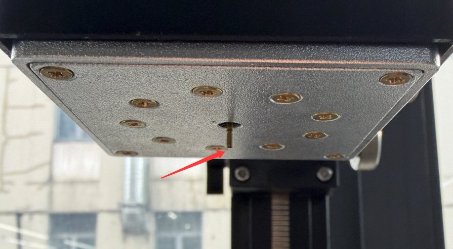
After each test, use a clean, soft cloth to wipe dust from the main unit’s exterior, the touchscreen, and the surface of the discharge tower to keep the equipment clean; use a dedicated screen-cleaning cloth to clean the touchscreen. Do not use organic solvents such as acetone, and do not spray water directly onto the screen to clean it; Clean dust and foreign objects from the surfaces of the test bench, sensing plate, and isolation plate weekly to ensure good insulation performance; if the probe tip is soiled, gently wipe it with a lint-free cotton swab dipped in a small amount of anhydrous ethanol, and allow it to air dry before use.
The probe can be unplugged directly for cleaning or replacement; see Figure 6-1.
6.2 Items for Periodic Inspection
6.2.1 Electrical Connection Inspection
Inspection Frequency: Once a month; Inspection Items: Check power cords, high-voltage cables, grounding wires, and communication cable connectors for looseness, oxidation, or damage; Remedial Actions: Tighten any loose connectors immediately; gently sand off any oxidation with fine-grit sandpaper; and replace any damaged cables immediately.
6.2.2 Mechanical Structure Inspection
Inspection Frequency: Once a month; Inspection Items: Check whether the test bench adjustment knobs turn smoothly, whether the probe bracket stop blocks are secure, and whether the probe extends and retracts normally; Remedial Actions: Apply a small amount of silicone grease to the adjustment mechanism for lubrication; replace the probe if it is deformed or worn.
6.3 Long-Term Storage Requirements
Before long-term storage, clean the entire surface of the unit and unplug all external cables; cover the unit with a dust cover and store it in a dry, well-ventilated environment free of corrosive gases; the storage environment should have a temperature of 0°C to 40°C and a relative humidity of ≤70%, and direct sunlight should be avoided; Every 3 months, power on the device and leave it in standby mode for 30 minutes to remove moisture and protect the high-voltage modules.
6.4 Persyaratan Interval Kalibrasi
Untuk memastikan akurasi pengukuran dan keandalan operasional peralatan, disarankan agar peralatan tersebut secara berkala dikirim ke laboratorium metrologi pihak ketiga yang berkualifikasi untuk kalibrasi. Interval kalibrasi yang disarankan adalah 12 bulan. Pengguna dapat menentukan interval kalibrasi spesifik berdasarkan frekuensi penggunaan, kondisi lingkungan, dan persyaratan sistem mutu.
7. Pemecahan Masalah dan Penyelesaian Masalah Umum
7.1 Kesalahan Terkait Daya
| Gejala Kesalahan | Kemungkinan penyebab | Prosedur |
|---|---|---|
| No display when powered on; power indicator light does not turn on | Kabel daya tidak terpasang dengan benar; sekring putus. | Check the power cord connections; replace the fuse with one of the same rating after turning off the power. |
| Touchscreen Not Responding | There are stains on the screen, and the system is malfunctioning. | Clean the screen surface; restart the device |
7.2 High-Voltage Faults
| Gejala Kesalahan | Kemungkinan penyebab | Prosedur |
|---|---|---|
| High voltage cannot be applied after clicking “Start.” | High-voltage cables not properly connected, poor grounding, and dirt on the test bench surface | After turning off the power, unplug and replug the high-voltage cables, then tighten them; check and secure the ground wire; clean the surface of the test bench. |
7.3 Operational Faults
| Gejala Kesalahan | Kemungkinan penyebab | Prosedur |
|---|---|---|
| Discharge cycles are not counted | The probe is not in contact with the device | Recalibrate the position to ensure good contact. |
| Communication error; the discharge tower is not operating | Kabel komunikasi yang longgar | Tighten the signal cable connections after power is turned off |
7.4 Waveform Anomalies
| Gejala Kesalahan | Kemungkinan penyebab | Prosedur |
|---|---|---|
| The waveform peak is too low | Poor probe contact, voltage set too low | Clean the probe tip and adjust the contact pressure; verify and increase the set voltage. |
| The rising edge of the waveform does not meet specifications | Probe wear, excessive ground loop impedance | Replace the test probe; check the ground wire and reduce the ground resistance. |
| Many waveform artifacts | Electromagnetic Interference from the Surroundings | Eliminate sources of interference and use shielded cables |